electronics assembly
The complexity and functionality of electronic devices often dictate the number of layers in an electronics assembly. From simple single-layer circuit boards to intricate multi-layer designs, the number of layers plays a crucial role in determining the device’s performance, reliability, and manufacturing cost. Understanding the factors that influence the layer count provides insight into the design and optimization of electronic assemblies for various applications.
At its core, a printed circuit board (PCB) serves as the foundation for mounting and interconnecting electronic components in an electronics assembly. The layer count of a PCB refers to the number of conductive layers sandwiched between insulating layers, known as the substrate. Each conductive layer contains copper traces that carry electrical signals between components, while the insulating layers provide mechanical support and electrical isolation between the conductive layers.
Single-layer PCBs, also known as single-sided PCBs, consist of a single conductive layer on one side of the substrate. These simple PCBs are often used in low-cost, low-complexity applications where space and manufacturing cost are not significant constraints. Single-layer PCBs are commonly found in consumer electronics such as calculators, remote controls, and basic household appliances.
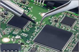
How many layers does an electronics assembly typically have?
As electronic devices become more complex and compact, multi-layer PCBs are increasingly prevalent in modern electronics assemblies. Multi-layer PCBs contain two or more conductive layers interconnected by vias, which are plated holes that allow electrical connections to pass between layers. Multi-layer PCBs offer several advantages over single-layer designs, including higher routing density, improved signal integrity, and reduced electromagnetic interference (EMI).
The layer count of a multi-layer PCB can vary depending on the device’s requirements and complexity. For example, a two-layer PCB consists of a top and bottom conductive layer separated by a single insulating layer, while a four-layer PCB adds two additional conductive layers for increased routing density and signal integrity. High-performance electronics assemblies, such as smartphones, tablets, and network switches, often utilize six or more layer PCBs to accommodate the dense circuitry and high-speed signaling requirements.
The layer count of a PCB is determined by several factors, including the device’s functionality, signal integrity requirements, size constraints, and manufacturing cost considerations. Increasing the number of layers allows for more intricate routing of signals, reducing signal crosstalk and improving noise immunity. However, adding layers also increases manufacturing complexity and cost, as each additional layer requires additional processing steps and materials.
Furthermore, the layer count of a PCB influences the assembly process and reliability of the electronic device. Multi-layer PCBs require specialized fabrication techniques, such as sequential lamination and controlled impedance routing, to ensure uniformity and consistency across all layers. Additionally, the increased complexity of multi-layer PCBs can make inspection and testing more challenging, requiring advanced inspection techniques such as X-ray inspection and automated optical inspection (AOI) to detect defects and ensure quality.
In conclusion, the layer count of an electronics assembly varies depending on the device’s requirements and complexity. While simple single-layer PCBs are suitable for basic applications with low-cost and low-complexity requirements, multi-layer PCBs are essential for high-performance electronics assemblies that demand dense routing, high-speed signaling, and robust reliability. By understanding the factors that influence layer count, manufacturers can optimize their designs and manufacturing processes to create electronic devices that meet the desired performance, reliability, and cost targets.