Achieve Dimensional Stability in Via Filling
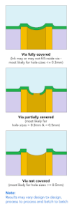
A via is a copper-plated hole that creates an electric connection between different layers on the PCB. During the PCB fabrication process, the via hole is plated and filled with either conductive or non-conductive material. The benefit of via filling is that it prevents impurities from entering the hole during soldering, improves mechanical strength, helps with component placement and strengthening pad attachment, reducing silkscreen printing issues, shortens signal paths and reduces the risk of solder wicking. Conductive via filling can be done with either a conductive epoxy or metal, such as silver or copper. The conductive filling is deposited by syringe or stencil printing and then cured.
Non-conductive via filling can be done with a variety of materials. In most cases, we use non-conductive epoxy paste. These are applied with syringes or stencils and then cured to solidify. Non-conductive filled vias do not transfer heat or signals. They are mostly used to stop solder or other impurities from entering the via hole during assembly. They also offer structural support for a copper pad that, in the case of a via-in-pad, covers the hole.
There are a number of considerations to keep in mind when designing a circuit board with via holes. The size of the via hole, how it is oriented on the board, and the drill-to-finished size ratio should all be carefully evaluated to make sure that the proper performance requirements are achieved.
Another important consideration is the metallization scheme. The correct selection of a copper plating thickness will help to ensure that the via hole has sufficient conductivity and current capacity. The choice of an appropriate plating solution is also important, as is the use of annular rings when possible.
How to Achieve Dimensional Stability in Via Filling
Voids can occur in the PCB manufacturing process when the plating solution is not properly agitated or monitored. To minimize the chance of voids, we recommend that you work closely with your PCB manufacturer to ensure that the proper conditions are in place for an optimal via filling process.
In addition to ensuring that all of the conductive or non-conductive materials are deposited in a consistent and reliable manner, it is essential to use proper soldering techniques. The right mix of temperature, time and pressure will help to produce a good quality joint that is strong and durable. We also recommend using a good quality soldering paste that is matched to the copper plating and the board technology for best results. In addition, we suggest that you use a high quality, low-sulfur solder. This will significantly decrease the oxidation rates, and it is much safer than standard tin-lead.
Additionally, via filling can enhance the mechanical strength of PCBs, reducing the risk of via barrel cracking or solder joint failure. This is particularly beneficial in applications subject to mechanical stress or thermal cycling, such as aerospace and defense electronics.
In summary, while rigid PCBs provide the basic framework for electronic circuits, via filling offers a means to enhance performance and reliability, especially in high-frequency and high-speed applications. By understanding the differences between these technologies, designers can choose the most appropriate approach to meet their specific design requirements.