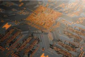
applications of stacked microvias in hdi pcb
Stacked microvias are a critical component of High-Density Interconnect (HDI) Printed Circuit Boards (PCBs), offering numerous advantages that make them well-suited for a variety of advanced applications across various industries. These tiny vias, which are stacked on top of each other within the PCB substrate, play a key role in enabling the miniaturization, high performance, and reliability of modern electronic devices.
One of the primary applications of stacked microvias in hdi pcb is in facilitating higher routing densities and increased interconnect complexity. By stacking multiple microvias on top of each other, designers can achieve greater routing flexibility and optimize signal paths between densely packed components. This allows for the creation of more compact and highly integrated PCB layouts, enabling the development of smaller and lighter electronic devices without compromising functionality or performance.
Moreover, stacked microvias are commonly used to improve signal integrity and minimize electromagnetic interference (EMI) in high-speed and high-frequency applications. By reducing the length of signal paths and minimizing the number of vias required for interconnections, stacked microvias help mitigate signal distortion, impedance variations, and crosstalk, ensuring reliable signal transmission and reception. This makes them ideal for applications such as telecommunications, data networking, and high-performance computing, where signal integrity is critical.
What are the applications of stacked microvias in hdi pcb?
Additionally, stacked microvias are well-suited for implementing complex routing schemes and advanced PCB architectures in HDI designs. Their small size and high aspect ratio allow designers to route signals between multiple layers of the PCB, enabling the creation of intricate signal paths, blind vias, and buried vias. This flexibility in routing enables the integration of additional components, functionality, and features into the PCB, making it suitable for a wide range of applications across industries such as aerospace, automotive, medical, and consumer electronics.
Furthermore, stacked microvias play a crucial role in enabling the integration of embedded passive components directly into the PCB substrate. By stacking multiple microvias around embedded components such as resistors, capacitors, and inductors, designers can create compact and highly integrated circuits that offer improved performance, reliability, and space efficiency. This integration of passive components reduces the need for discrete components, simplifies assembly, and enhances overall system reliability, making it ideal for applications where size, weight, and reliability are critical factors.
Another important application of stacked microvias in HDI PCBs is in thermal management and heat dissipation. With the miniaturization of electronic devices and the increasing power densities of modern components, efficient heat dissipation is essential to prevent thermal issues and ensure the reliability of the PCB. Stacked microvias act as conduits for heat transfer between different layers of the PCB, allowing for more efficient thermal spreading and dissipation. This helps prevent thermal hotspots, improves component reliability, and extends the lifespan of electronic devices, particularly in applications with demanding thermal requirements.
In conclusion, stacked microvias are versatile components that find wide-ranging applications in HDI PCBs across various industries. From enabling higher routing densities and improved signal integrity to facilitating complex routing schemes, embedded components, and thermal management solutions, stacked microvias play a crucial role in the design, performance, and reliability of modern electronic devices. As technology continues to advance, the applications of stacked microvias in HDI PCBs will only continue to expand, driving innovation and pushing the boundaries of what is possible in electronic engineering.