Benefits Does HDI Technology Offer
The HDI is a measure of how well people are living in countries. It includes factors such as life expectancy, GDP per capita and education levels. However, critics say that the HDI ignores trade-offs and overstates a country’s performance. They also argue that the measure correlates poorly with other highly correlated values such as energy use and economic development.
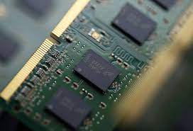
Due to their smaller dimensions, shorter length and lower number of layers, high density interconnect PCBs require less raw material than traditional printed circuit boards (PCBs). They also save on production costs because they require fewer stages to manufacture. A single HDI board can replace multiple traditional PCBs in a device, saving money and space.
This is achieved by using smaller pads, copper traces and vias. This makes it possible for designers to place components closer together which reduces the number of connections and the overall size of the board. This leads to a significant reduction in overall signal loss and crossing delays.
Additionally, the buried vias and staggered or stacked microvias of HDI PCBs enable the conductors on different layers to be interconnected freely. This allows the shortest paths between components, which in turn improves electrical performance.
Lastly, the HDI technology allows the circuit boards to be more compact and lightweight. This is especially important for mobile devices such as tablets and smartphones. It also allows for more features to be packed into a small space, thereby improving the functionality and usability of these products.
What Cost-Saving Benefits Does HDI Technology Offer?
To achieve this, the stack-up of an HDI PCB is composed of various laminates separated by partially cured prepregs. The individual layers are pressed and heated to liquify the prepreg, then the stack-up is bonded together through sequential laminations. The process is repeated until the required design is achieved and then the etched copper layers are laminated to the prepregs.
The types of vias, through-holes or microvias used in an HDI PCB will impact the cost. Smaller and more complex vias, as well as more layers in the design, will drive up the cost. The number of sequential laminations in the PCB is also an influencing factor as it adds to the manufacturing time and cost.
In addition, a standard via formation process is needed to produce HDI PCBs with filled plated microvias. This is known as the via-in-pad process and involves placing a pad on a flat land, then plating it, filling it with one of several different fill types, capping it, and then plating over it. This is a time-consuming and expensive process and is best reserved for high-reliability applications.
Another option is to use a near-pad technique, where a very short trace section comes off from the pad and touches the microvia. This completes the connection to an internal layer and provides a larger breakout channel should drill wander cause any deviation from the desired drill hit location. This approach is more reliable than microvias and can help reduce failure rates.