How Is Rigidity Controlled in Rigid Flex Design?
In the field of electronics, rigid flex PCBs (Printed Circuit Boards) have gained prominence due to their ability to combine the benefits of both rigid and flexible circuit technologies. These boards offer significant advantages in compact, high-performance devices like wearables, medical devices, and automotive applications. However, one of the critical aspects of rigid flex design is controlling the rigidity of the board to ensure it performs optimally under various mechanical and electrical conditions. Properly managing rigidity in rigid flex design ensures that the flexible sections maintain their ability to bend without compromising the stability and functionality of the rigid parts. Let’s explore how rigidity is controlled in rigid flex design.
1. Material Selection
The rigidity of a rigid flex PCB begins with material selection. The materials used for both the rigid and flexible parts of the PCB play a significant role in determining the overall rigidity of the board. The rigid sections are typically made from materials such as FR4, a fiberglass-reinforced epoxy laminate that provides excellent mechanical strength and electrical insulation. On the other hand, flexible sections are typically made from materials like polyimide, which are highly flexible and resistant to heat.
The key to controlling rigidity in rigid flex design lies in selecting the appropriate material for each section. The rigid areas need to be thick enough to support components and prevent deformation, while the flexible areas must have a thinner, more pliable construction that allows them to bend and conform to the desired shape. By adjusting the thickness and composition of these materials, engineers can control the rigidity and flexibility balance across the entire board.
2. Layer Stack-up Configuration
The way the layers of the rigid flex PCB are stacked and bonded together also plays a crucial role in controlling rigidity. A typical rigid flex design will consist of alternating layers of rigid and flexible materials. By varying the number of layers and how they are stacked, designers can control the rigidity of the overall board.
For example, the rigid sections can be made thicker with more layers to provide additional strength and support, while the flexible areas are kept thinner. Engineers may also add reinforcement in specific areas of the flexible sections by using additional layers or stiffeners, which are rigid materials placed strategically to provide localized rigidity where needed.
Layer stack-up configurations are a critical part of the design process for rigid flex boards, as they influence both the mechanical strength of the rigid areas and the flexibility of the flexible areas. Fine-tuning the stack-up ensures the board performs as required for its specific application, whether that means achieving a high degree of flexibility in certain sections or maximizing rigidity in others.
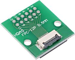
3. Use of Stiffeners
Stiffeners are an essential component of rigid flex design, particularly in areas that require extra rigidity. These are additional layers of rigid material, such as FR4, that are bonded to the flexible sections to provide mechanical support. Stiffeners are commonly used in areas where components need to be mounted or where the PCB must resist bending during assembly or usage.
By controlling the placement and thickness of stiffeners, designers can fine-tune the rigidity of specific areas of the rigid flex board. For example, if a particular flexible section of the board needs to be more rigid to support heavier components, a thicker or more strategically placed stiffener can be used. Conversely, if greater flexibility is required in certain regions of the board, the stiffeners can be minimized or avoided altogether.
The use of stiffeners allows designers to selectively control the rigidity of the rigid flex PCB, ensuring that each area of the board has the right balance of flexibility and stability for its intended function.
4. Controlled Bending Zones
In rigid flex design, controlling where and how the board bends is essential to maintaining the functionality and longevity of the circuit. Engineers can design controlled bending zones by defining specific areas where the flexible sections of the PCB are intended to bend. These areas are carefully designed with optimized trace routing and minimal stress points to allow the board to flex without damaging the circuitry.
By precisely engineering the bendable regions of the rigid flex PCB, designers can ensure that the rigid sections remain stable while the flexible sections perform their intended function. Controlled bending zones are particularly useful in applications like foldable devices, where repeated bending is a key characteristic of the product’s design.
5. Testing and Simulation
Once the design of the rigid flex PCB is complete, the rigidity must be tested and simulated to ensure that the board will perform as expected under real-world conditions. Computer-aided design (CAD) tools and simulations allow engineers to model the rigidity of the board and simulate how it will react to various stresses, such as bending, twisting, or thermal expansion.
Simulation tools can identify areas where rigidity may be insufficient, allowing designers to adjust the material selection, layer stack-up, or stiffener placement before moving to production. Rigorous testing and simulation ensure that the rigid flex PCB performs reliably and that the rigidity is controlled to meet the specific needs of the device.
6. Manufacturing Precision
The precision with which the rigid flex PCB is manufactured also plays a crucial role in controlling its rigidity. Any variations in the thickness of the rigid or flexible materials, misalignment during layer bonding, or imprecise stiffener placement can affect the overall rigidity of the board. Therefore, it is essential that the manufacturing process be tightly controlled to ensure that the design specifications are met.
Using advanced fabrication techniques and automated processes, manufacturers can ensure that the rigid flex PCB is produced with the desired rigidity and flexibility characteristics. High precision in manufacturing helps eliminate potential issues such as warping or uneven bending, resulting in a more reliable and functional board.
Conclusion
Controlling rigidity in rigid flex design is a delicate balance between flexibility and strength. By carefully selecting materials, configuring layer stack-ups, using stiffeners, designing controlled bending zones, and utilizing testing and simulation tools, designers can ensure that the board has the right amount of rigidity for its intended application. Rigidity is a key factor in ensuring that rigid flex PCBs perform reliably in demanding environments while maintaining their flexibility and compact design. Properly controlling rigidity allows rigid flex technology to meet the needs of modern electronics, from wearables to aerospace applications.